Hydrogel Microneedle Fabrication: Femtosecond Laser Solution for Sub-micron PDMS Structure Etching
Transdermal drug delivery systems (TDDS) have emerged as a pivotal focus in phar...
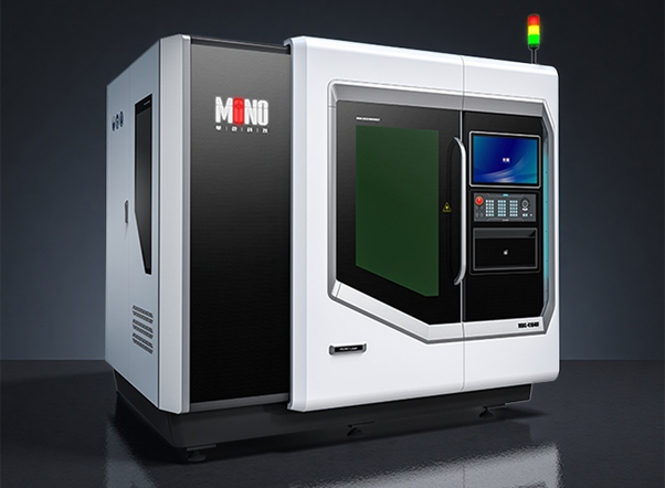
MONO | 2025-05


INDUSTRY
The escalating import costs and restricted supply of crucial equipment like lithography machines and etching tools have created an urgent demand for breakthrough technologies and alternatives. This need extends across the entire semiconductor industry chain, especially when it comes to the core components used in the testing process.

The test probe market is segmented into various sub - sectors, including semiconductors, PCBs, and ICT in - circuit testing, based on their applications. Among these, semiconductor test probes present the highest technical hurdles. Their manufacturing is incredibly challenging due to the need for extreme precision in dimensions, along with complex electrical and mechanical performance requirements.
Challenges in Semiconductor Test Probe Manufacturing
Semiconductor test probes are minute yet vital precision electronic components. Despite differences in appearance depending on their functions, they typically consist of a tip, a shaft (or a more complex structure incorporating a spring and a sleeve), with overall dimensions often in the micron range. These probes play a crucial role in semiconductor chip design verification, wafer testing, and final product testing. Acting as a connection between the chip's pins or bump bonds and the testing equipment, they accurately transmit signals to evaluate the chip's performance metrics.
Microstructure processing at a scale as small as a grain of rice or even smaller is no easy feat. What's more, ensuring that the processed probes possess excellent electrical conductivity (low contact resistance), mechanical strength (high resistance to bending), and high wear resistance (long service life) adds another layer of difficulty. Conventional manufacturing methods, such as lithography combined with chemical etching or precision stamping, encounter complex procedures and high costs when aiming for micron - level precision. When dealing with high - hardness or specialized materials like tungsten, tungsten steel, and palladium alloys, these methods often result in issues like rough contact surfaces, residual burrs, material deformation caused by stress, and poor tip shape control. These flaws directly impact the accuracy and reliability of probe testing, posing a significant challenge to the yield and cost control within the semiconductor industry.
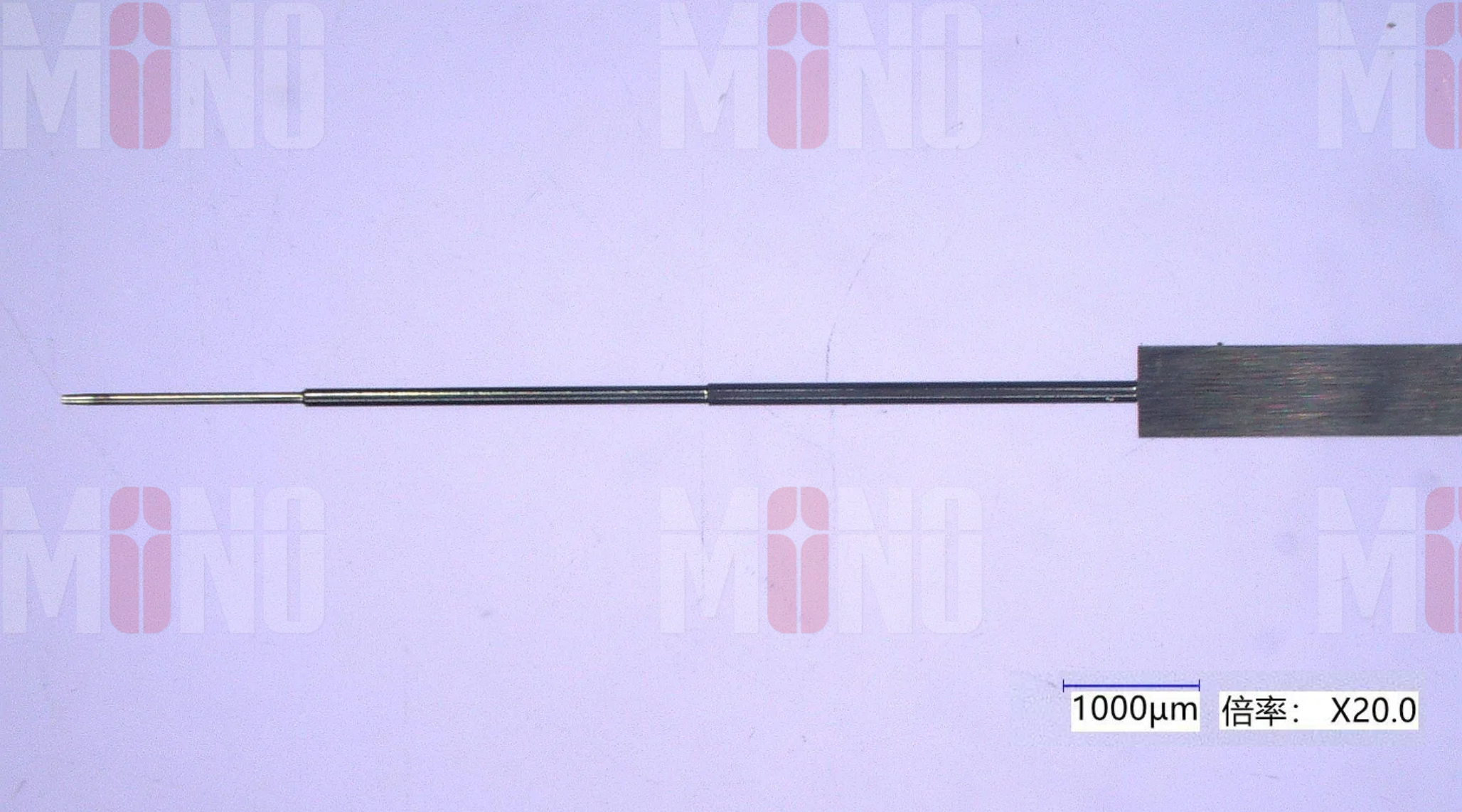
Is there a way out? Currently, femtosecond laser processing technology has emerged as a promising solution. Take a 0.1 - mm - thick tungsten steel probe as an example. When cut using femtosecond laser technology, the top width can be precisely controlled within 110.7μm±1μm. The process is stress - free and deformation - free, and the surface roughness is as low as Ra≤0.1μm, highlighting the remarkable micro - machining capabilities of femtosecond lasers for high - hardness materials.

Advantages of Femtosecond Laser Cutting
how does the femtosecond laser manage to achieve such outstanding results?
1. Non - damaging "Cold" Cutting: The pulse width of a femtosecond laser, which is in the order of 10⁻¹⁵ seconds, is significantly shorter than the heat transfer time within the material. This means that the laser energy acts on the material surface instantaneously, vaporizing and removing the material without generating a significant heat - affected zone. Whether it's high - hardness and high - melting - point materials like tungsten and tungsten steel or other metals, ceramics, and polymers, femtosecond lasers can perform high - quality "cold" cutting, leaving no recast layer, micro - cracks, or heat - induced deformation. This is essential for preserving the original physical properties of the probe material, ensuring stable electrical conductivity and a long mechanical lifespan during testing.
2. Ultra - precise Micro - machining: Femtosecond laser beams can be focused down to the micron or even sub - micron level. Paired with a high - precision motion control system, it can achieve a processing accuracy of ±1μm or even higher. The non - contact nature of laser processing means it's not restricted by the shape of traditional cutting tools. By precisely controlling the beam path, it can cut complex 2D and 3D probe structures with rib widths as narrow as just a few microns. This makes it an ideal choice for new product R & D and small - batch, multi - variety production scenarios.
3. Superior Cutting Edge Quality: The quality of the probe's contact end face and edges has a direct impact on the stability of the contact resistance and the probe's lifespan. Femtosecond laser - cut edges are smooth, with excellent perpendicularity (either no taper or a controllable taper), and a roughness of Ra≤0.1μm, with almost no burrs or slag. This not only improves the contact stability and durability of the probe but also eliminates the need for complex post - processing steps such as deburring and polishing.

Looking ahead, the industrial application of femtosecond laser technology is set to expand further. This technological innovation offers new hope for overcoming the manufacturing challenges of key components like high - end test probes, and it will undoubtedly contribute to strengthening the resilience and competitiveness of the semiconductor industry chain.